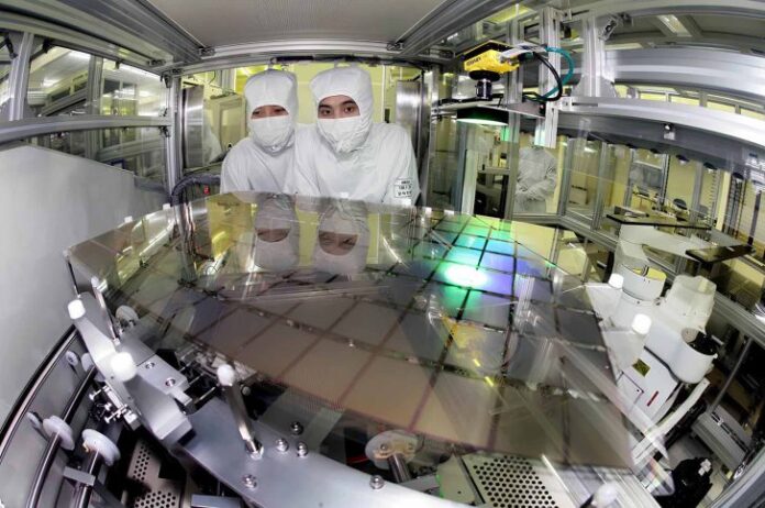
Samsung has been reported on a few occasions to be struggling with its 3nm GAA yields, and while the logical move might have been to find ways to improve that percentage, the Korean foundry is making a monumental leap towards mass producing its 2nm node. However, according to one update, the company is not actually pursuing the production of 2nm wafers but has labeled its second-generation 3nm technology with the same name. Naturally, this can cause confusion for Samsung’s clients and mislead them into thinking that they are receiving wafers on a cutting-edge manufacturing process. Samsung’s first 2nm order supplied […]
Read full article at https://wccftech.com/samsung-2nm-process-renamed-2nd-generation-3nm-node/
WccftechContinue reading/original-link]


